PCB
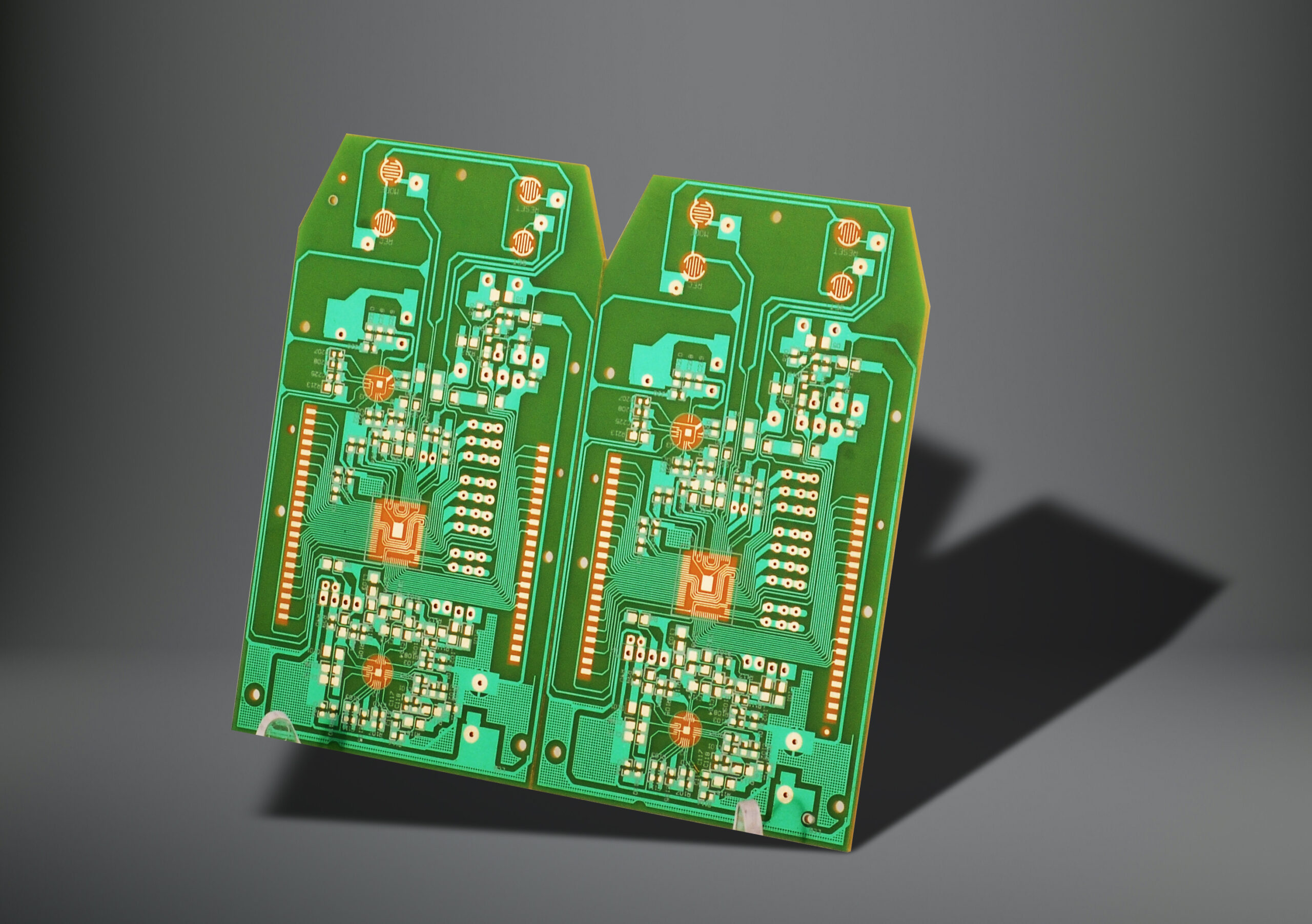
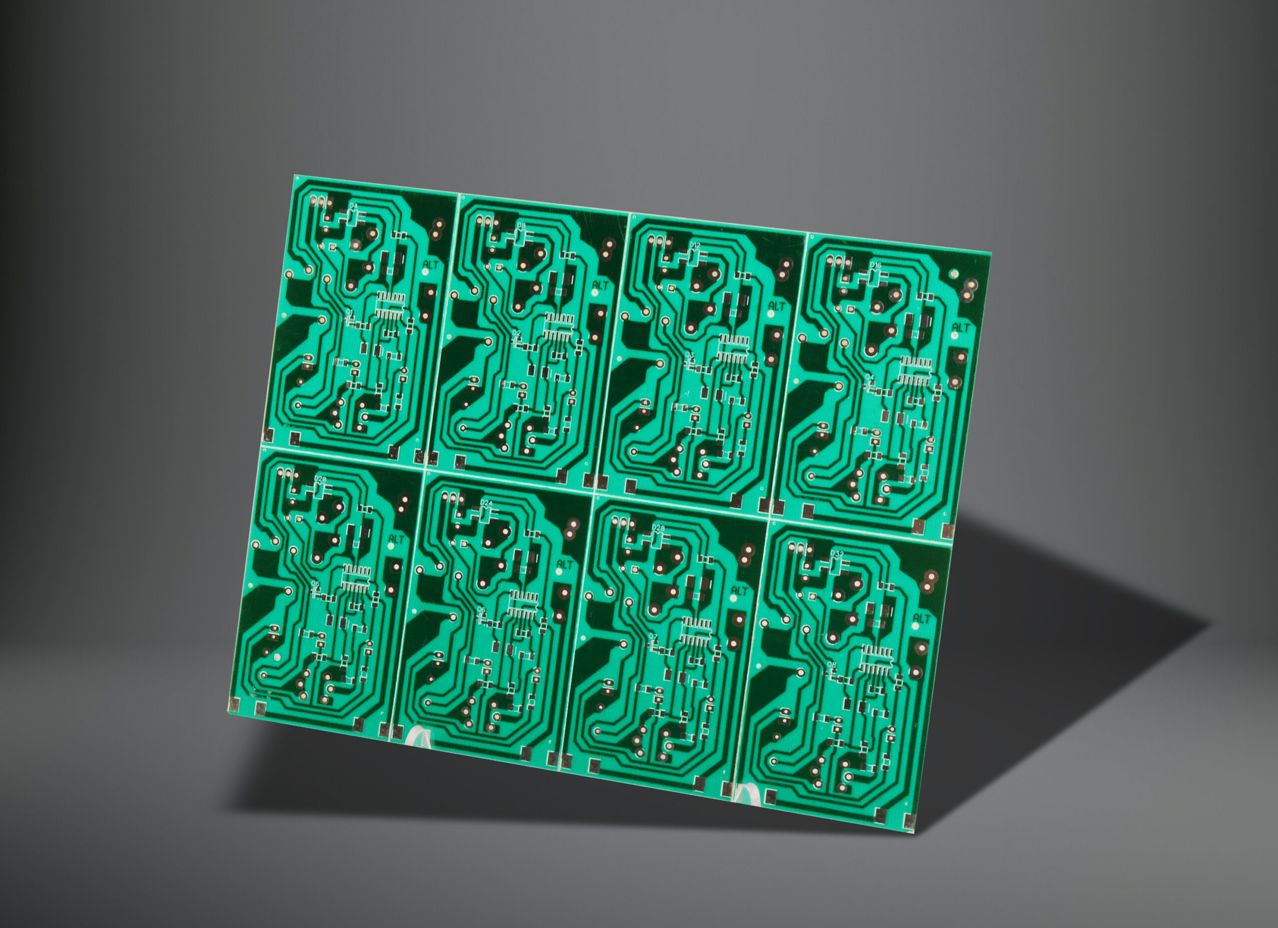
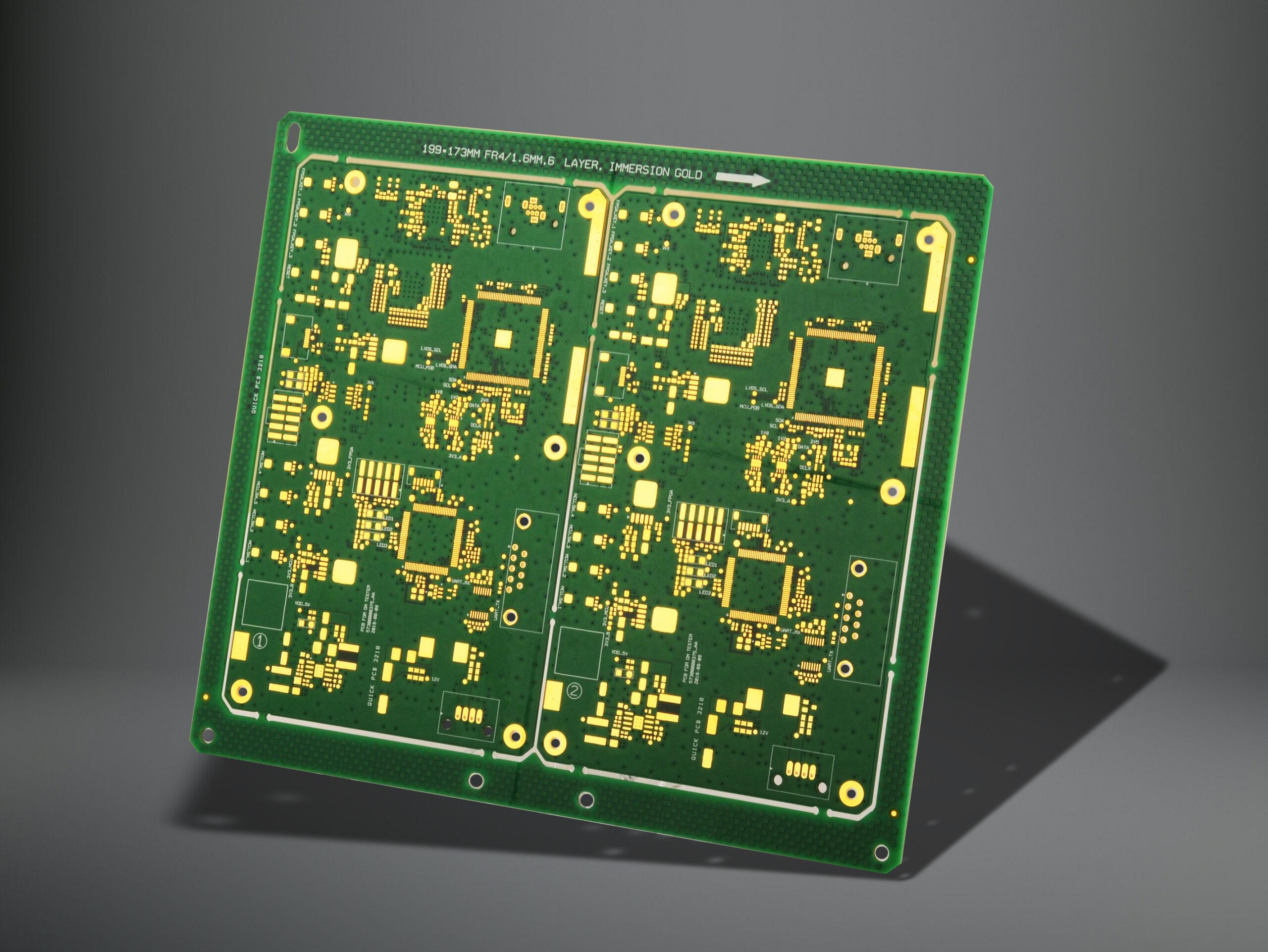
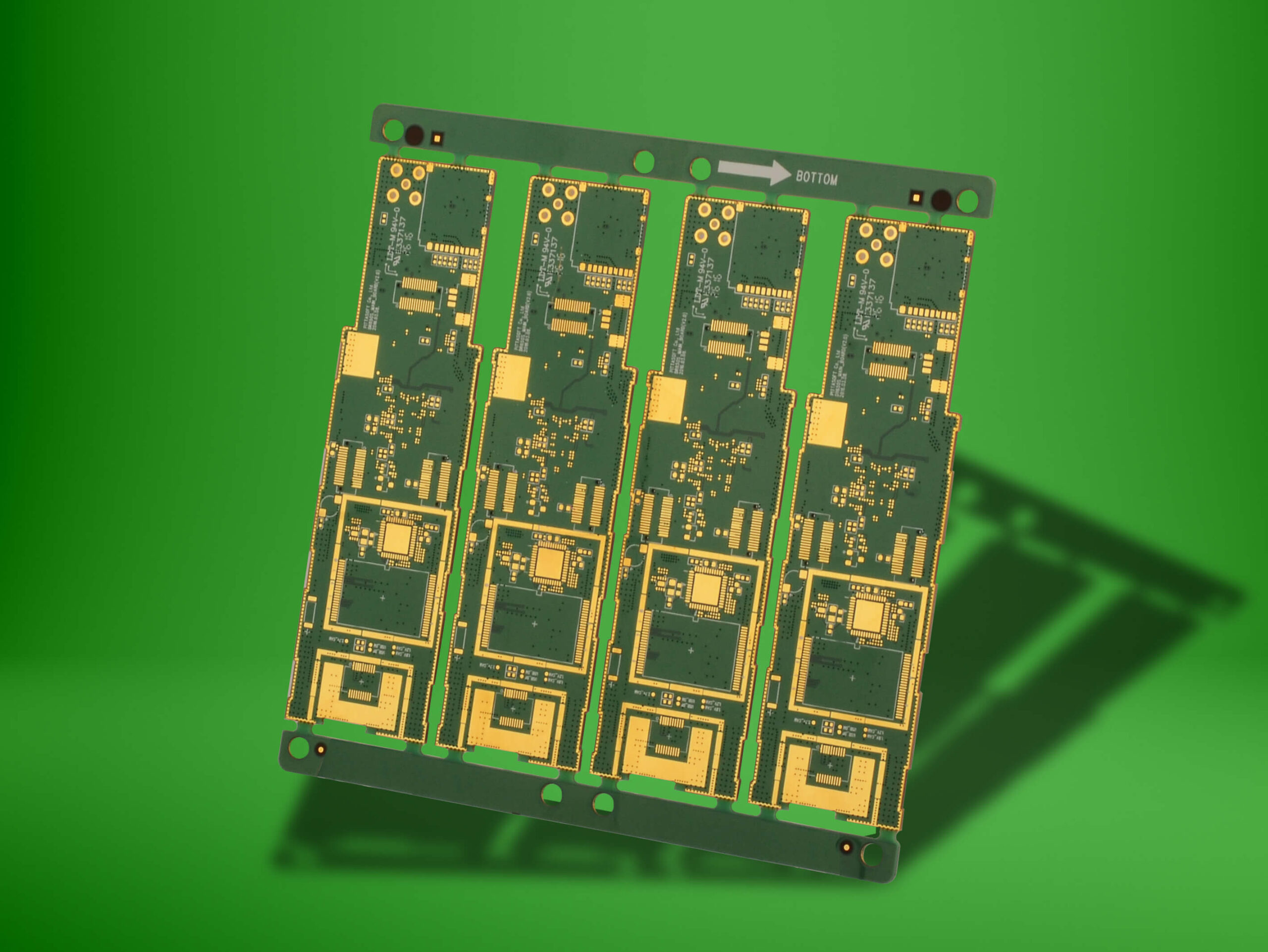
Our company supplies a wide range of Printed Circuit Boards (PCB) to its customers. We strive to meet the diverse needs of our customers by providing them with high quality PCBs for their various applications.
| Parameter | Mass Production | Prototype Production |
| Layer Count | 1-18 Layer PCB | 1-56 Layer PCB |
| Raw Material | FR-4, Metal-Based PCB (Aluminum, Copper, etc.), HDI, High TG, Teflon CEM-1, CEM-2, CEM-3, Rogers, Polyimide Flex (PI), PET (Transparent) |
FR-4, Metal-Based PCB (Aluminum, Copper, etc.), HDI, High TG, Teflon CEM-1, CEM-2, CEM-3, Rogers, Polyimide Flex (PI), PET (Transparent) |
| Max. Panel Size | 600*770 mm (23.62″ x 30.31″) for 2L+, 500*1200 mm (19.69″ x 47.24″) for 1L | 600*770 mm (23.62″ x 30.31″) for 2L+, 500*1200 mm (19.69″ x 47.24″) for 1L |
| Max. PCB Thickness | 8.5 mm | 8.5 mm |
| Min. PCB Thickness | 2L: 0.3 mm | 2L: 0.1 mm |
| 4L: 0.4 mm | 4L: 0.3 mm | |
| 6L and above: 0.8 mm | 6L and above: 0.8 mm | |
| Min. Inner Layer Clearance | 3 mil | 3 mil |
| Min. Trace Width | 3/3 mil | 3/3 mil |
| Min. Trace Spacing | 3/3 mil | 3/3 mil |
| Min. Hole Diameter | 0.1 mm | 0.1 mm |
| Min. PTH Thickness | 25 μm | 25 μm |
| Min. Blind/Buried VIA Size | 0.1 mm | 0.1 mm (1-18 Layer) |
| PTH Diameter Tolerance | ±0.076 mm (±3mil) | ±0.076 mm (±3mil) |
| NPTH Diameter Tolerance | ±0.05 mm (±2mil) | ±0.05 mm (±2mil) |
| Hole Position Deviation | ±0.05 mm (±2mil) | ±0.05 mm (±2mil) |
| Thick Copper Options | 6 OZ/175 μm | 13 OZ/455 μm |
| Min. S/M | 0.1 mm (4mil) | 0.1 mm (4mil) |
| Solder Mask Color | Green, Blue, Red, White, Black, Matte Green, Matte Black, Purple | Green, Blue, Red, White, Black, Matte Green, Matte Black, Purple |
| Legend Ink Color | White, Black, Yellow, Red, Gray | White, Black, Yellow, Red, Gray |
| Surface Finish | HASL, Lead-Free HASL, ENIG, OSP, Hard Gold, ENEPIG, Immersion Silver, Immersion Tin, None (Bare Copper) | HASL, Lead-Free HASL, ENIG, OSP, Hard Gold, ENEPIG, Immersion Silver, Immersion Tin, None (Bare Copper) |
| Routing Methods | CNC Routing, V-Groove, Beveling Punch, Chamfering | CNC Routing, V-Groove, Beveling Punch, Chamfering |
| Routing Tolerance | Up to 1.0 mm: ±0.1 mm, Above 1.0 mm: ±0.15 mm (±6mil) | Up to 1.0 mm: ±0.1 mm, Above 1.0 mm: ±0.15 mm (±6mil) |
| Peelable Mask | Top, Bottom, Double-Sided | Top, Bottom, Double-Sided |
| VIA Techniques | Tented, Open, Plugged, Pad-in-Via, Filled Via (Resin Filled) | Tented, Open, Plugged, Pad-in-Via, Filled Via (Resin Filled) |
| Advanced Features | Half Plated Hole, Halogen-Free, Edge Plating, Special Stack-Up Press-Fit Hole, Carbon Ink, Via Plugged with Copper Cap, Black Core Material |
Half Plated Hole, Halogen-Free, Edge Plating, Special Stack-Up Press-Fit Hole, Carbon Ink, Via Plugged with Copper Cap, Black Core Material |
| Impedance Control | ± 10% | ± 7% |
| Insulation Resistance | 1×10¹² Ω (Normal) | 1×10¹² Ω (Normal) |
| Hole Plating Resistance | <300 Ω (Normal) | <300 Ω (Normal) |
| Thermal Endurance | 3×10 sec@288℃ | 3×10 sec@288℃ |
| Bending/Flexing Tolerance | ≤0.7% | ≤0.7% |
| Electric Strength | >1.3 KV/mm | >1.4 KV/mm |
| Peel Strength | 1.4 N/mm | 1.4 N/mm |
| Solder Mask Abrasion Resistance | >6H | >6H |
| Flammability | 94V-0 | 94V-0 |
| Test Voltage Value | 50-330V | 50-330V |


